
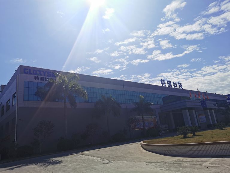
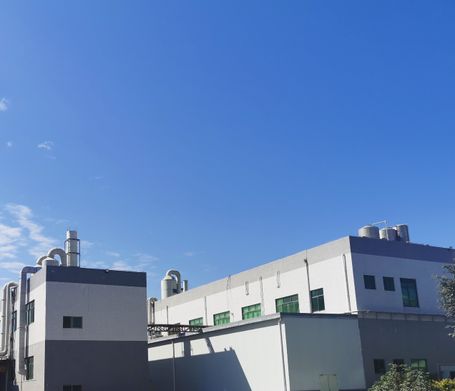
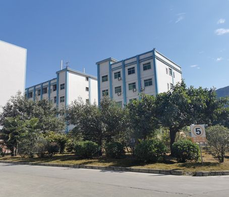
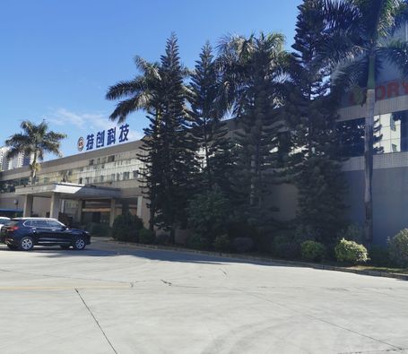
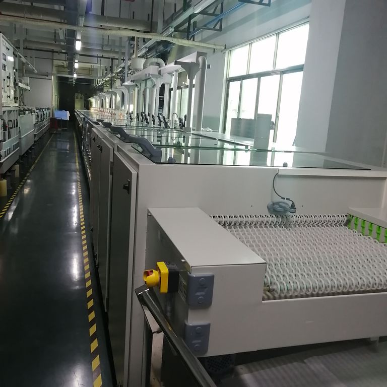
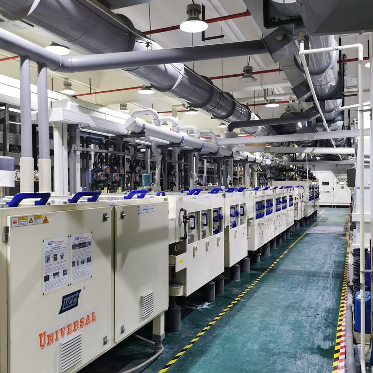
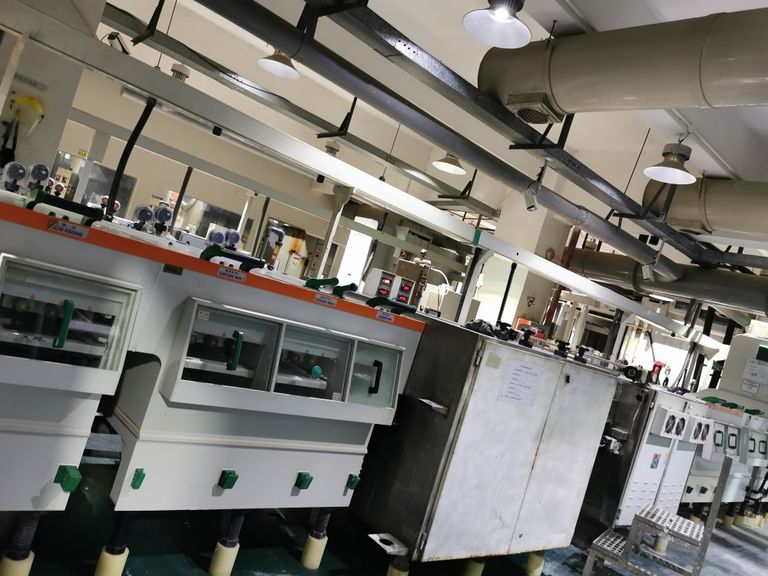
Glorysky factories
Factories in Huizhou Glorysky
Huidong plant I
Construction area 40,000 ㎡
Staff 700
Main products ::>4L 、 High Frequency,
High speed boards
Monthly capacity 50.000㎡
Order Structure Multi layer high mix, low volume
Huidong Plant II
Construction area 40,000 ㎡
Staff 200
Main products Aluminum based,
copper based boards & SS boards
Monthly capacity 50,000㎡
Order Structure IMS, SS in mass
production
Factories in Huai'an Glorysky
Huai'an Plant I
Construction area 36,000 ㎡
Staff 600
Main products: Consumer Electronics, LCD, Storage
Monthly capacity 80,000㎡
Order Structure Mass production
Huai'an Plant II
Construction area 150,000 ㎡
Staff 2000
Main products Consumer electronics, LCD, Mini-LED, Storage
Monthly capacity 150,000㎡
Order Structure: Mass production
Factories in HuBei Glorysky
In constructing

Our Management
Glorysky Group is led by a highly experienced team with an average of 30 years in global PCB production industry. The General Manager Paul Li is one of the most worldwide acknowledged PCB Experts in Taiwan Region with highly extensive PCB knowledge both in technology and in production. Glorysky management team consists of the CEO, the CFO, business leaders, functional heads and the leaders for the different regions.
25+years accumulated automotive know-how experts Team
With the average of more than 25 years in automotive know-how in the world key PCB industy in Taiwan Region and in global PCB Companies, our professional team of experts will supervise and follow every process and stage of your unique project and application requirement.

Our Capabilities
Technical Capability -multi layer Printed Circuit Board
Parameter 2019 2020 2021
Layer 26 32 40
Working Panel size 1050mm*610mm 1200mm*610mm 1500mm*610mm
Max. board thickness 4.0mm 6.0mm 8.0mm
Min.board thickness 0.5mm 0.4mm 0.3mm
Min.core thickness 0.076mm 0.05mm 0.05mm
Max. finished copper thickness 6OZ 10OZ 12OZ
Min.LW /LS 0.076/0.076mm 0.076/0.076mm 0.06/0.06mm
Min.hole diameter of 0.2mm 0.2mm 0.15mm
mechanical drilling
Min.hole diameter of laser drilling 0.1mm 0.1mm 0.076mm
Inner- layer 0.2mm Inner-layer 0.18mm Inner-layer 0.18mm
Min.PAD Out-layer 0.2mm Out-layer 0.18mm Out-layer 0.18mm
Distance from hole side to hole
side(different nets) 0.275mm 0.25mm 0.25mm
Aspect ratio 10:1 12:1 15:1
Impedance tolerance ±10% ±8% ±8%
Special technology 1 step HDI 2 step HDI 3 step HDI
POFV separated gold finger rigid flex
copper in lay back drilling High speed backplane
mixed lamination
Our Capabilities
Technical capability high-frequency, high-speed
Capability item Technical data R&D/samples manufacture remark
High-frequency PTFE PTFE+Ceramic, PTFE+ FR4 Ceramic, PTFE+ FR4
Min, max. board mm Max4.5 Min 0.2 Max4.0 Min 0.3
thickness max. layer 26 20
Working Panel size mm Max1000*550 Min 50*50 Max1000*550 Min 100*100
Outline Dimension Outline accuracy/mm +/-0.05 +/-0.1
slots Slot size accuracy/mm Normal slot+/-0.08 Normal slot+/-0.1 Short slot
short slot+/- 0.1 short slot+/-0.13 length/width ≤2
Interlayer alignment Distance from min. hole to
ability conductor/mm 0.2 0.25
Lamination Mixed lamination with different PTFE+Hydro ceramic+ Fr 4 PTFE+Hydro ceramic+Fr 4
capability materials
Min. hole diameter/mm 0.3 0.35
Hole treatment Min. hole wall distance/mm 0.6 0.65 Different net holes capability Hole diameter tolerance/mm PTH +/-0.08 NPTH:+/-0.05 PTH+/-0.1 NPTH:+/-0.05
Hole location tolerance/mm Size: 200*200 +/-0.08 Size: 200*200+/- 0.1
plating ratio 15:1 10:1
Homogeneity COV≤5% COV≤7%
Resin plugging ratio 12:1 10:1
Hole types via+blind holes via+blind holes
Line width Line width accuracy/mm +/-0.015 +/-0.025
Impedance control Impedance tolerance(≥50Ω ) +/-8% +/-10%
planeness Bow and twist 0.5% 0.75%
Sueface finish types ENIG/immersion tin/hard gold plating/soft gold plating/OSP/HALLF/HA
Our Capabilities
Technical capability--IMS
items 2019 2020
max layer SS, 2L with alu aside, 2L alu in the middle DTP, mixed lamination
Base materials FR4、 CEM1 、 CEM3 1 5 series aluminum, copper based BT,ceramic boards
Thermal conductivity 1W、 2W 、 3W 、 4W 、 5W 、 8W
Aluminum suppliers Bergquist, Ventec ,, SY 、 Polytronics , Boyu , ITEQ,Chin shi , Chuanghui, Alliance Huazheng
Board thickness 0.6mm~3.2mm Min:0.4mm Max:4.0mm
Finished board thickness 0.5oz~6oz Max:8 oz
Dielectric thickness 50mm~200um
Hole diameter tolerance (NPTH) ±0.075mm ±0.05mm
Outline profiling Laser routing, punching , CNC, V CUT Outline
Outline tolerance punching ±0.10 mm CNC ± 0.150mm CNC±0.10mm
Finished size (max ) 350*1500mm
Surface finish HASL, HALLF, OSP, ENIG, immersion tin, immersion siilver
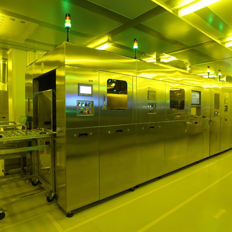
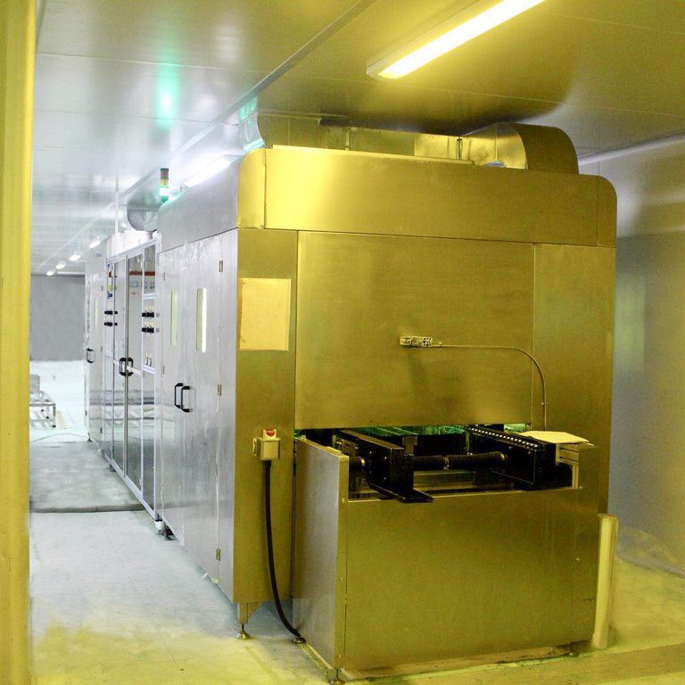

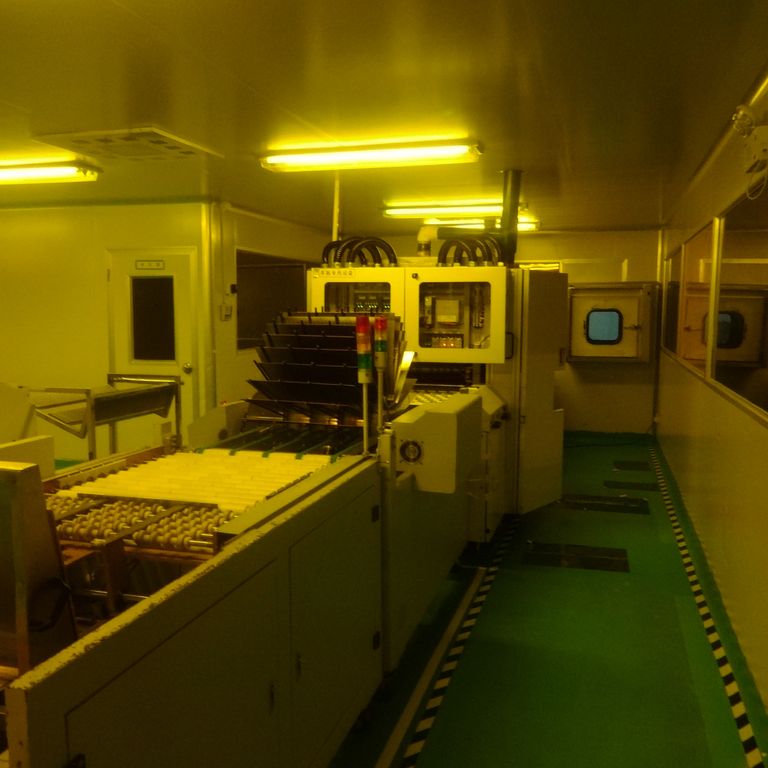
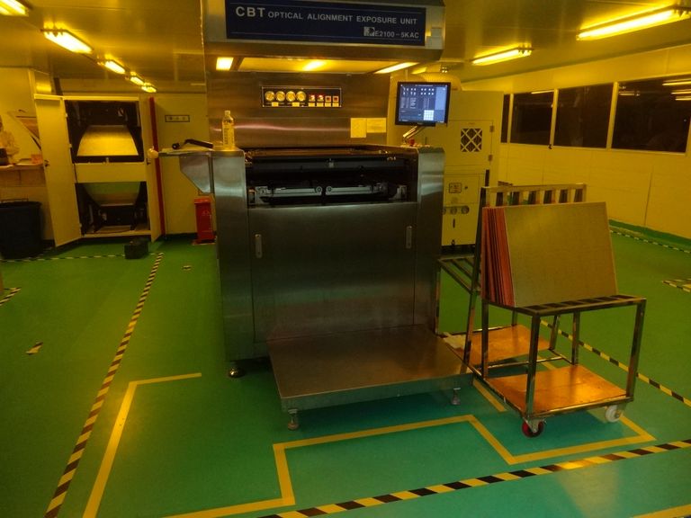
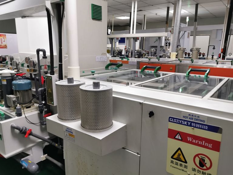
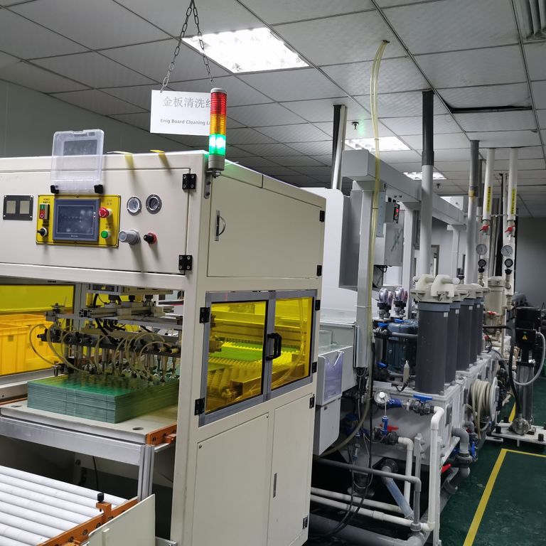
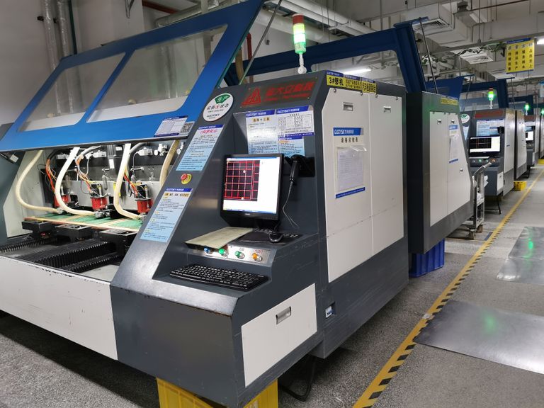
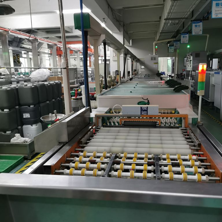
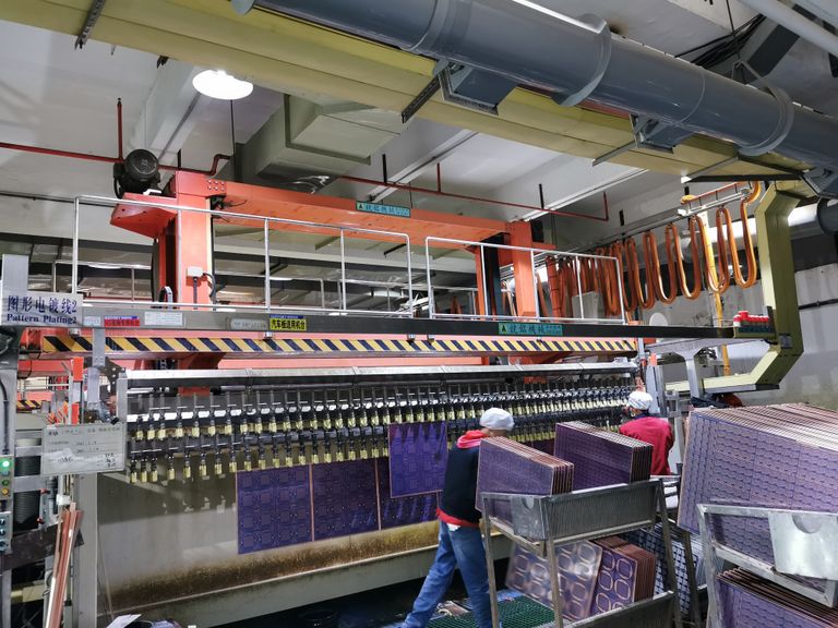
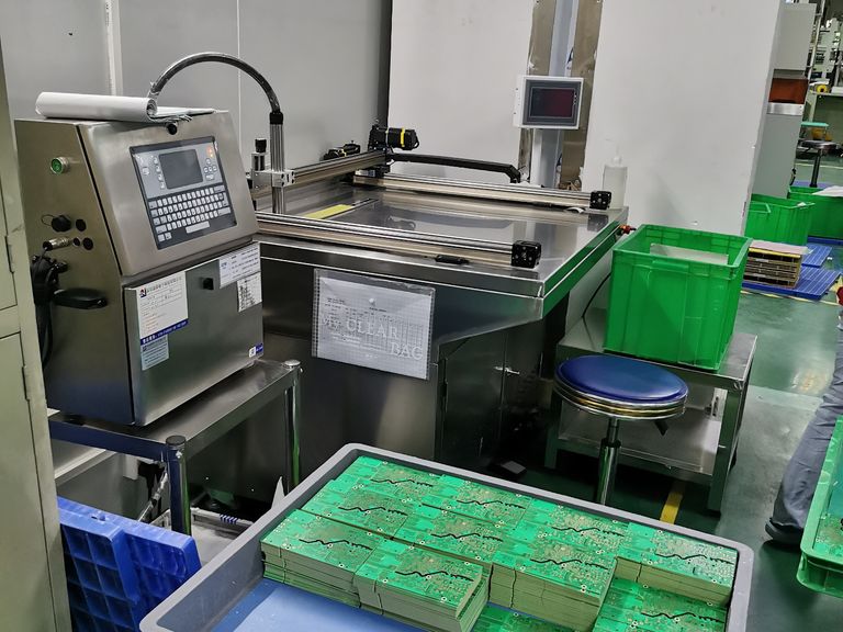
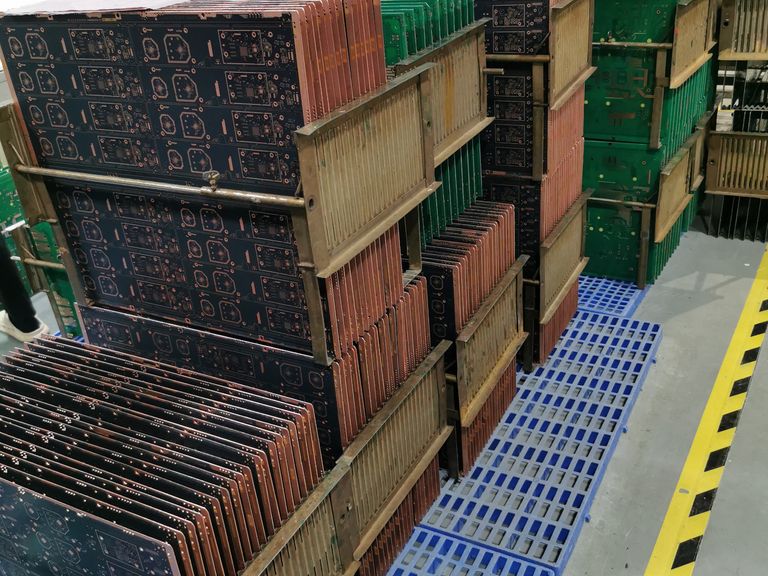
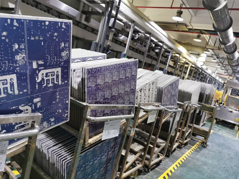
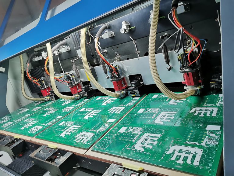
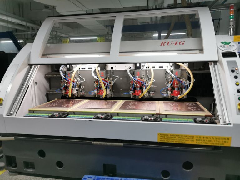
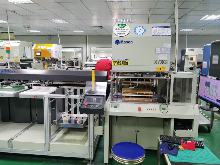
Product in Processing

We are the leading PCB manufacturer and provide our global customers with our secure and reliable solutions for any PCB requirement.
Copyright © 2015 Glorysky Electronics Co.,Ltd., All rights reserved. ICP Number :13001567